General Group Overview
The advancement in semiconductor materials, devices and fabrication techniques has been one of the most important driving forces for the ever-changing Information Age and the Internet of Things (IoT). My research has focused on semiconductors to make smaller, faster, lower-cost and more energy efficient computation and communication hardware.
Research Areas
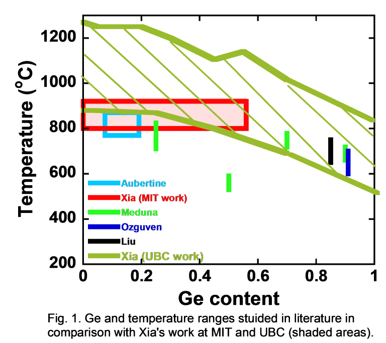
Group IV semiconductors in microelectronics (since 2000)
To further advance the performance of microelectronic devices such as CMOS and HBTs, group IV elements and alloys such as germanium (Ge), SiGe, SiGe:C and GeSn are integrated into silicon platforms to boost performance by stress, bandgap and defect engineering. The integration of these new materials, especially with the increasing Ge, Sn or C fractions and the resulting stresses, introduces new process phenomena and fabrication challenges such as dopant diffusion and segregation, Si-Ge interdiffusion, Ge-Sn interdiffusion, stress-diffusion interaction etc. We investigate these new phenomena experimentally, catch them in mathematical models and implement in TCAD simulation tools to assist industry in structure and fabrication design of these devices.
Our Si-Ge interdiffusion data and models have been widely used and implemented in the state-of-the-art process simulation tools including Intel R&D’s in-house process simulation tool, Crosslight Software’s CSUPREMTM and Synopsys’s Sentaurus ProcessTM (the leading commercial 3D process simulation tool in the semiconductor industry), and Lumerical’s DEVICETM for structure and process design of next generations of semiconductor device. Our work on dopant profile engineering has been used extensively by the Analog Technology team of Texas Instruments.
Si-compatible lasers (since 2008)
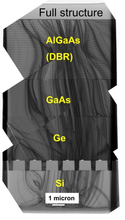
Fig. 2. Transmission electron microscopy image of the DBRs on ART-Ge/Si substrates. Wavy lines are due to sample thickness variations.
Integrating optical functions with Si-based microelectronics has been a long dream for the semiconductor industry to reduce cost and increase packaging density.
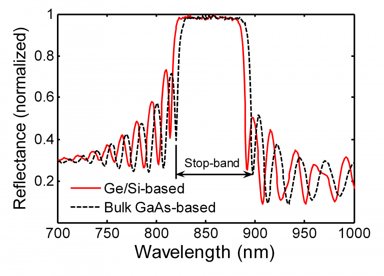
Fig. 3. Normal-incidence reflectance spectra of bulk GaAs-based DBRs and ART-Ge/Si-based DBRs normalized by the maximum intensity. The difference is within cross-sample uniformity.
A major challenge in realizing this dream has been in finding Si-compatible light sources, especially lasers. Our work first demonstrated the successful integration of AlGaAs distributed Bragg reflectors (DBRs) on on-axis Si (100) substrates via a Ge layer formed by aspect ratio trapping (ART) technique (Fig. 2). The DBRs were grown by LandMark, our supporting organization in Taiwan. The GaAs/ART-Ge/Si-based DBRs have reflectivity spectra comparable to those grown on conventional bulk GaAs substrates (Fig. 3) and have smooth morphology, good periodicity and uniformity. Anit-phase domain formation is significantly reduced in these substrates, and threading dislocation density of the GaAs layer shown was 105 to 6 × 106 cm-2. These paved the way for the successful full VCSEL growth and fabrication on GaAs/ART-Ge/Si substrates. We are currently working on full VCSELs on GaAs/Ge/Si substrates in collaboration with Prof. Chiao-hsin Wu at National Taiwan University and LandMark Optoelectronics.
Our recent work studied the impacts of dopants and annealing on Si-Ge interdiffusion and the Ge film quality for Ge-on-Si structures including surface roughness, etch pit density, interdiffusion and photoluminescence with the collaboration with Prof. Jifeng Liu (Dartmouth College) and Dr. Kwang Hong Lee and Prof. Chuan Seng Tan (Nanyang Technological University). The un-annealed P or As-doped Ge films have similar photoluminescence intensity at a 25% doping concentration and smoother surface compared with the first Ge laser work by MIT in 2012, which are promising for Ge lasers with better light emission efficiencies.
On the device modeling and simulation side, we focused on addressing the potential and optimization of Ge-on-Si lasers with 2D stress and laser modeling and simulations. Ge-on-Si lasers are another important option for Si-compatible lasers with the advantages of easy integration and fabrication with Si-based microelectronics and thus much lower fabrication cost and shorter time to deployment. Our studies showed that with laser structure optimization and stress engineering, a wall-plug efficiency of 30% can be achieved with currently available Ge growth techniques, which are tremendous improvements from the available experimental value of about 0.1%. Considering that common commercial compound semiconductor lasers have wall-plug efficiencies in the range of 20-30%, our studies strongly support Ge-on-Si lasers and gave guidance for future improvements.
GaN power devices (since 2017)
AlGaN/GaN-based high electron mobility transistors (HEMTs) have been under extensive research for their high breakdown voltage, good thermal stability and low noise performance. We investigate multiple aspects of GaN HEMTs including approaches in realizing enhancement-mode GaN HEMTs and in forming low resistance contacts. These efforts are in collaboration with Prof. Hongyu Yu at South University of Science and Technology, China and Enkris Semiconductor, China.
2D semiconductors (since 2015)
2D semiconductors are suitable for thin, quasi-transparent and flexible electronics and photonics. Black phosphorus was successfully isolated in 2013 and was shown to have unique properties such as direct and tunable bandgap from 0.3 to 2 eV, suitable for applications in thermal imaging, photovoltaics and telecom. We investigate the fabrication and properties of single to few-layer black phosphorus and MoS2.
With a new polycarbonate-film-based dry transfer method, we successfully fabricated twisted stacked few-layer black phosphorus. Optical characterization showed the overlapping area had special optical response, and high frequency Raman spectroscopy showed an abnormal blue shift in Ag1 and Ag2 modes. Density functional theory (DFT) calculations confirmed this blue shift in twisted bilayer black phosphorus, and revealed significant interlayer coupling effects. Charge distribution calculations indicated weak valence bond may exist between the two layers. This finding may lead to applications in phonon modulation and gate switchable transportation.
3D integration of ICs (since 2012)
Through-silicon-via (TSV) is a key element for 3-D integration in providing vertical interconnects for chip-stacking structures. Thermal-mechanical stress originating from the thermal expansion coefficient mismatch of Cu and Si can cause uniformity and reliability issues. We study the stress distribution around Cu-filled and carbon-nanotubes-filled TSVs, its influencing factors and the impact on carrier mobility and keep-out zone (KOZ) for logic devices near the TSVs, which is important for the design and reliability of 3D integrated circuits. These efforts are in collaboration with Prof. Chuan Seng Tan at Nanyang Technological University.
Raman spectroscopy (since 2011)
Micro-Raman spectroscopy is a powerful tool in studying chemical concentration, stress, crystallinity, chemical bonding, and temperature. We have the capability of doing in-situ Raman during thermal treatment. The material systems we are interested in include SiGe:C alloys, Ge nanowires, InGaAs/GaAs, carbon nanotubes, graphene, nanocrystalline Si, black phosphorus, FinFETs, Ti oxide and soils.
Projects
- Enhance-mode GaN HEMTs with metal/2D material gates
- La-based GaN S/D contacts and gate contacts
- i-GaN and MIS-gate for GaN HEMTs
- Vertical doping profile control for PNP and NPN SiGe HBTs
- Doping effects on Si-Ge interdiffusion and on epitaxial Ge film quality
- Fabrication and Raman response of twisted stacked few-layer black phosphorus
- Stress engineering and fabrication of Ge-on-Si lasers
- Stress field around Cu and CNT-filled TSVs
Experimental Facilities
- High resolution confocal micro-Raman LabRam HR by Horiba Scientific
- AMPEL nanofabrication facility
Computational facilities and specialized software packages
- TSUPREM-4, Medici, Sentaurus Process by Synopsys
- LASTIP, CSUPREM, APSYS by Crosslight Software
- INTERCONNECTS by Lumerical Solutions
Faculty